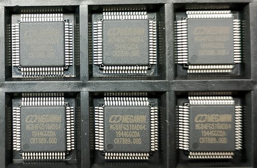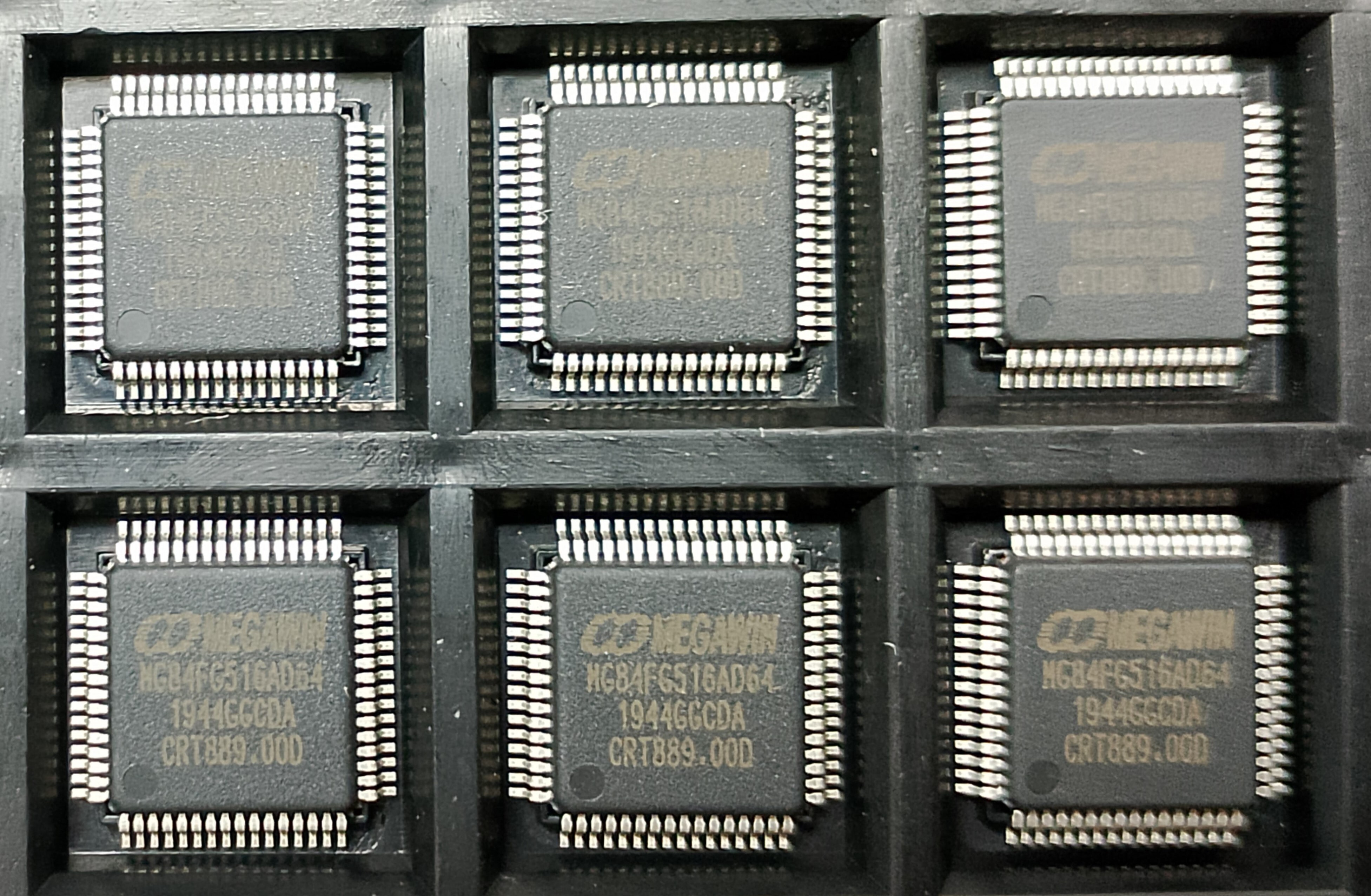


MG84FG516AD64 USB IC
Product Details:
MG84FG516AD64 USB IC Price And Quantity
- 140.00 - 150.00 INR/Piece
- 145 INR/Piece
- 10 Pcs Piece
MG84FG516AD64 USB IC Trade Information
- Cash Against Delivery (CAD) Cash Advance (CA) Cash in Advance (CID)
- All India
Product Description
1-T 80C51 Central Processing Unit
* MG84FG516 with 64K Bytes flash ROM
*ISP memory zone could be optioned as 1KB/1.5KB4KB
*Flexible IAP size.
*Code protection for flash memory access
*Flash erase/program cycle: 10,000 times
*Flash data retention: 100 years at 25ï
* Data RAM
*On-chip 256 bytes scratch-pad RAM
*4096 bytes expanded RAM (XRAM)
*Up to 5120 bytes expanded RAM (XRAM) by sharing USB buffer
* Dual data pointer
* Variable length MOVX for slow SRAM/Peripherals
* Interrupt controller
*17 sources, four-level-priority interrupt capability
*Four external interrupt inputs, nINT0, nINT1, nINT2 and nINT3
*All external interrupts support High/Low level or Rising/Falling edge trigger
* Four 16-bit timer/counters, Timer 0, Timer 1, Timer 2 and Timer 3
*T0CKO on P34, T1CKO on P35, T2CKO on P10 and T3CKO on P01
*X12 mode enabled for T0/T1/T2/T3
* Programmable 16-bit counter/timer Array (PCA) with 6 compare/capture modules
*Capture mode
*16-bit software timer mode
*High speed output mode
*8/10/12/16-bit PWM (Pulse Width Modulator) mode with phase shift function
* Keypad Interrupt (P0/P2/P5/P6)
* 12-Bit ADC
*Programmable throughput up to 250 ksps
*Up to 8 channel single-ended inputs or 4 channel differential inputs
* Enhanced UART (S0)
*Framing Error Detection
*Automatic Address Recognition
*Speed improvement mechanism (X2/X4 mode)
* Secondary UART (S1)
*Dedicated Baud Rate Generator
*S1 shares baud rate generator to S0.
* Master/Slave SPI serial interface
* Master/Slave tow wire serial interface (TWSI)
* USB Device Controller
*USB Full speed (12Mbps) operation and USB specification 2.0 compliant
*Intel 8X931 like USB control flow
*Built-in USB transceiver and 3.3V regulator
*Six pairs flexible endpoints for control/interrupt/isochronous/bulk IN/OUT transaction
*1K bytes FIFO for USB endpoint buffer
*Software-controlled USB connection/disconnection mechanism
* Programmable Watchdog Timer
*One time enabled by CPU or power-on
*Sourced from on-chip low frequency oscillator
*Interrupt CPU or Reset CPU on WDT overflow
*Watch mode support
* On-Chip-Debug interface (OCD)
* Maximum 55 GPIOs in LQFP64 package
*P3 can be configured to quasi-bidirectional, push-pull output, open-drain output and input only
*P0, P1, P2, P4, P5 and P6 can be configured to open-drain output or push-pull output
*P6.0 and P6.1 shared with XTAL2 and XTAL1
* Multiple power control modes: idle mode, power-down mode, slow mode, sub-clock mode, watch mode and monitor mode.
*All interrupts can wake up IDLE mode
*12 sources to wake up Power-Down mode
*Slow mode and sub-clock mode support low speed MCU operation
*Watch mode supports WDT to resume CPU in power down
*Monitor mode supports BOD1 to resume CPU in power down
* Two Brown-Out Detectors
*BOD0: detect 2.2V
*BOD1: selected detection level on 4.2V/3.7V/2.4V/2.0V
*Interrupt CPU or reset CPU
*Wake up CPU in Power-Down mode
* Operating voltage range: 2.0V ï 5.5V
*Minimum 2.2V requirement in flash write operation (ISP/IAP/ICP)
* Operating frequency range: 36MHz(max)
*External crystal mode, 2 ï 12MHz @ 2.0V ï 5.5V and 2 ï 25MHz @ 2.7V ï 5.5V.
*CPU up to 12MHz @ 2.0V ï 5.5V, up to 25MHz @ 2.4V ï 5.5V and up to 36MHz @ 2.7V ï 5.5V
* Clock Sources
*Internal 12MHz oscillator (IHRCO): factory calibrated to 1%, typical
*External crystal mode
*Internal Low frequency RC Oscillator (ILRCO) support: about 32KHz
*External clock input (ECKI) on XTAL2/P6.0, up to 36MHz.
*Internal Oscillator output on XTAL2/P6.0
*On-chip Clock Multiplier (CKM) to provide high speed clock source
* Operating Temperature:
*Industrial (-40ï to +125ï)*
Other Products in 'Semiconductor IC' category
 |
RKSEMITRONICS
All Rights Reserved.(Terms of Use) Developed and Managed by Infocom Network Private Limited. |

 Send Inquiry


